

- Bez kategorii (21)
- Codes Scratches (4)
Atmega8 Frequency counter
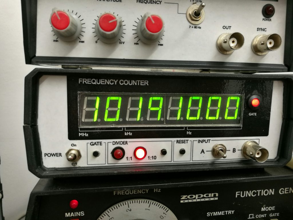
A few years ago (4-5?) I bought a ZOPAN KZ1405 frequency generator, and after a few weeks of using it I noticed that the lack of digital readout is a real pain in the ass. Besides, , it is a really old piece of equipment and to get into spec it needs about 45 minutes to get “warm”, and stabilize itself. So I sat down and started drawing a draft of a small frequency counter. The idea was to create something relatively simple, just to orientate oneself in the real frequency on f-gen output.
Plans and concept
The main idea was to create something simple. It was to be based on Atmega8 MCU, have something to multiplex its output for segments led display, some external clock for better frequency stability (than the crystal and the capacitors connected to atmega). And finally a simple divider on input, to extend the range of inputs signal up into 10MHz. Oh! And ofcrz a selectable gate timing.
Scheme showing how it works
Below you can find the scheme.
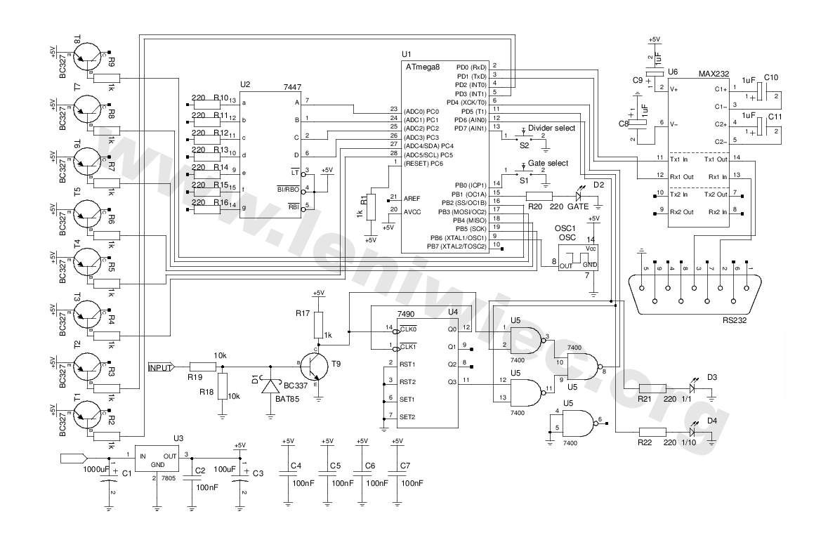
Let’s start talking about how it works… The input signal is provided into a simple amplifier, based on T9, R1, R18, R19 and D1 elements. This amplifier works as a simple signal shaping circuit providing output signal proper for digital circuits inputs. The signal from its output (a T9 collector) is provided into the CLK0 input of the 7490 counter, which is implemented as a frequency divider, with a ratio of 1:10.
From the Q3 output the signal is provided into the NAND gate U5 (we have here a TTL chip, 7400 – quadruple nand gate). The circuit made of three logic gates (NAND) from the U5 works as a switch, which is driven by a logic signal from U5 mcu, PD5 (pin 11) and PD6 (pin 12). This signals determine what we have on the output of our switch circuit – the signal from Q3 (pin 11 – U4), or straight from the T9-based amplifier.
And so, if we have a high logic level on PD5 and a low logic level on PD6, then we also have a high level on input A (pin 13) nand gate. And on its output we get a negated signal from the B input (pin 12). The second nand gate (pin: 1,2,3 – U5) has a low logical level on the input A (pin 2), and in this situation, whatever logical state we put on its B input (pin 1), we will always get a high level on the output. The outputs of both of the gates are connected to two inputs of the third nand gate. And if one of this inputs is in a permanent high level, and the second one gets some signal, we will get on its output (pin 8) a negated signal that we provide to this second input. So, on the output of the third gate (pin 8), we will get exactly the same signal as it is on the circuit input A (pin 12). If we reverse the situation, and we put a high level on PD6 of U1, and a low one on PD5, then the situation will be exactly opposite, and we will get exactly the same signal on the output of the third gate (pin 8), as it is on the input B of the first gate (pin 1). Therefore we can select from which input we want to get the signal into T0 input of U1.
Additionally, two LED D3, D4 and their current limiting resistors R21,R22 were connected to PD5 and PD6 to signal the selected divider. And these are, basically, all the input circuits. The U1 mcu is additionally equipped with a few other external components: an external clock generator OSC1, the PB1 configured as input are connected to a led diode D2 (with the corresponding limiting resistor), which signalises gate actions. The PB0 (configured as input) is connected to a S1 switch (a gate timing set button), and similarly, the PD7 is connected to a S2 switch (a divider select button). Both S1 and S2 are internally pulled-up, and the debouncing is software-implemented. The reset input (pin 1) is connected to + by R1 (yeap, I know, I know, it is not the world’s best solution for a reset circuit…).
Next, we have the ports PC0…PC3, which drive the BCD code encoder to a 7-segment led display, whose outputs are connected in parallel to all eight led displays. Each of the eight displays refreshes separately, one by one, and is driven by the transistors T1…T8.
Display
It works in such a way that the number we want to display on the eight positions is broken down to each individual digit, and each of these digits are sequentially converted into BCD code, and sent to PC0..PC3 of U1. In the same time, the PC4,PC5, PB5, PB4, PB3, PB2 outputs drive the corresponding digit on display. The whole process is continued until we get the last digit, then the display is cleared, and we start once again, refreshing it with a frequency that cannot be registered by a human eye.
Let’s look into the code that is responsible for all that.
void enableT(uint8_t x)
{
	PORTB |= (1 << PB2);
	PORTB |= (1 << PB3);
	PORTB |= (1 << PB4);
	PORTB |= (1 << PB5);

	PORTC |= (1 << PC4);
	PORTC |= (1 << PC5);
	PORTD |= (1 << PD2);
	PORTD |= (1 << PD3);


	if(x == 7)
		PORTB &=~(1 << PB2);
	else if(x == 6)
		PORTB &=~(1 << PB3);
	else if(x == 5)
		PORTB &=~(1 << PB4);
	else if(x == 4)
		PORTB &=~(1 << PB5);

	else if(x == 0)
		PORTC &=~(1 << PC4);
	else if(x == 1)
		PORTC &=~(1 << PC5);
	else if(x == 2)
		PORTD &=~(1 << PD2);
	else if(x == 3)
		PORTD &=~(1 << PD3);
} // end of enableT()

	while(1)
	{
	   …
	   enableT(n);
	   PORTC &= 0xF0; //clear last 4 bit
	   PORTC |= buff[7-n];//-'0';

	   if(n>=7)
		   n=0;
	   else
		   n++;
	   ...
	}
What we have here is an enableT() procedure and an infinite loop. The enableT() procedure gets one parameter, which is a number. This number determines which position on the display should be turned on. If we look inside the body of this procedure, we can clearly see that first all the outputs are cleared. Then the position which is equal to the input param is turned on. In the main loop (the infinite one), first we fire up the above procedure, which turns on the selected position on the display. Then we clear the last 4 bits of the port C, and assign the value from the buff table. In the next fields of the matrix we get the next digits from the number that we need to display. And this way, after eight loop executions, the whole display is refreshed.
Firmware
Besides the display handling, the firmware also contains the handling for the buttons and both counters are turned on. T0 as a counter, and T1 as a timer with the prescaler set to 256. T0 counts the impulses on MCU input. T1 is responsible for the gate. It works this way that each interruption generated by T0 increments the global variable ‘overflows’ by 1, and each interruption of the timer T1 (which is our gate) counts the number of the input impulses already registered, and respectively (depending on selected divider and gate time), multiplies the result and prepares the current measure of the frequency in the current_f variable. The content of this global variable is broken down into digits (buff matrix), and displayed on the led display. You may download the whole code and the ready-to-use bin/hex files, at the bottom of this post.
Programming the MCU
If you want to program your Atmega8, you need to remember that we do not use the crystal and the capacitor (we use external oscillator OSC1), and we need to set the corresponding fuse bit before we start to program our chip. In our configuration we will use an external clock, so the fuse will look like this:
LOW: 0xE0
HIGH: 0xD9
and if you use avrdude, here are the ready-to-use command line parameters:
-U lfuse:w:0xe0:m -U hfuse:w:0xd9:m
Summary
Below you can find a link to all available project files, including the pcb layout, the front panel layout, the code etc. The PCB is designed especially for the Z1 case, so the mounting holes are perfectly targeted into the mounting pillars of the Z1 case. If someone is interested in how I make my own pcbs with solder mask and silk screen, you can find out about it here: how I made my pcb with soldermask, and silk screen.